| Apr 2003 | VLSI Basics |
|
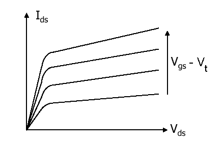
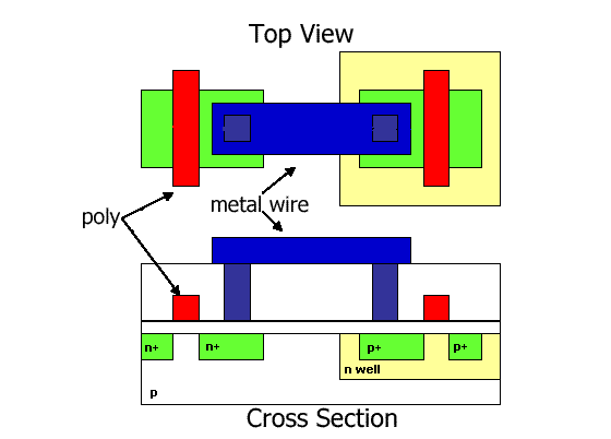
MOS transistor
Voltage on gate controls current that flows between source and drain.
Here is how transistor looks on layout. Drain and source are usually of green or yellow color,
gate is red. Transistor is formed when poly (red color) crosses diffusion layer.
VLSI Technology
PMOS technology based on p-MOS transistors was invented first.
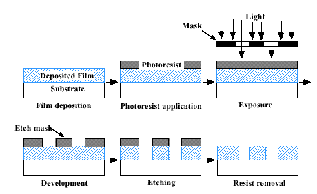
VLSI Fabrication A typical submicron CMOS process uses p-type wafers. A blank 8-inch wafer costs about $100. An IC fabrication process contains a series of masking steps to create layers that define the transistors and metal interconnect. Most layers are formed by the following steps: put layer, protect needed area with photoresist, apply light to transpose, remove photoresist and unprotected layer areas. This photolithografy process is illustrated on the image:
n-well and p-well are formed by ion implantation, when ions of dopped silicon n+ or p+ are forced into wafer area with a great speed. During the implantation the ions can get inside to a depth of a few microns. Further transistor layers are formed by diffusion (high T ion migration). Gates are created from poly (polycristalline silicon). Poly has to have a good conductance. To improve the coductance poly is covered with a silicide (a metallic compaund of silicon). SIO2 is an insulator, it also protects the outer layer from oxidation. Layers of poly and SiO2 can be deposited using chemical vapor deposition (CVD). Metal layers can be deposited using sputtering.All these layers are patterned using masks and photolithografy process. Power Consumtion
Static power consumption is defined by leakage.
Leakage is a junction currents caused by thermally generated carriers. Their value increases exponentially
with increasing junction T. For example, 85C (a common junction T) results in increase by a factor of 60
over room T.
References:
HITEQUEST Apr 2003 |