Flash is the next generation of EPROM, that was invented by Intel in the 1970's.
Flash - quickly erasable memory, became popular since 1990's.
Erasing information stored in flash is conducted by electrical process for less than 1sec, instead of the UV light illumination for 20min for EPROM.
EPROM has to have an expensive package with quartz window for erasing.
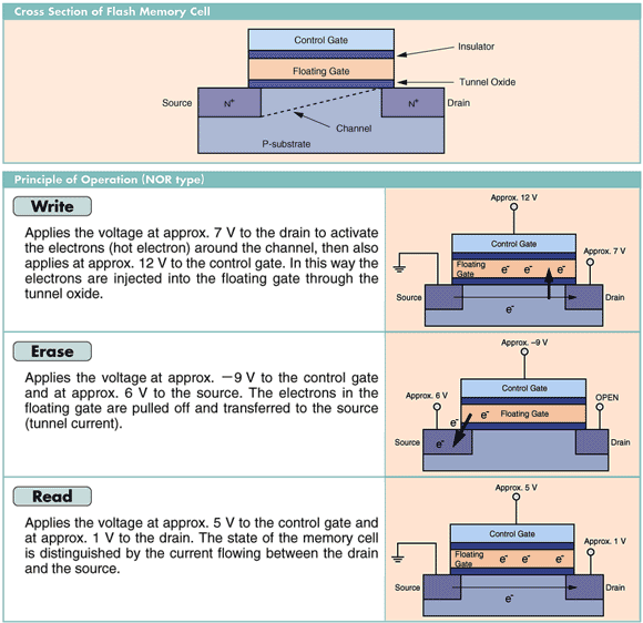
Flash basic element is a floating gate transistor.
It differs from normal transistor by having an extra, unconnected gate sandwiched between the normal (control) gate
and the channel region. Floating gate is isolated from above and below by thin oxide layers.
The operation of flash is based
on a process of removing (erase) or putting (program) electrons on the floating gate.
Charge on floating gate affects the threshold of the memory element.
When electrons are present on the floating gate, no current flows through the transistor, indicating logic 0. The transistor is
conducting, indicating logic 1, when electrons are removed from the floating gate.
The process of forcing electrons to/from floating gate is achieved by applying a voltage between a control gate and source or drain
and called Fowler-Nordheim (F-N) Tunneling.
Fowler-Nordheim (F-N) Tunneling
Tunneling is a process when electrons are transported through a barrier. For SiO2 with a 3.2 eV barrier a significant
tunnel current can be observed when the oxide thickness is reduced to less than 4nm.
For thicker oxide it is still possible to have a significant tunnel current when a high field of >10 MV/cm is applied
across the oxide. The tunneling process in oxide was reported by Fowler and Nordheim .
Example of flash array configuration.
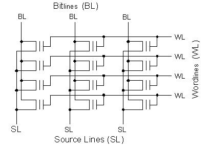
WL (word line) is the horizontal line and BL (bit line) is the vertical line. Control gates are connected to WL,
where the decoded address is applied. BL connects drains together and represent data bus, SL connects sources to common ground.
The voltage combination applied to WL and BL define an operation: read, erase or program.
Again, the operation of flash is based
on a process of removing (erase) or putting (program) electrons on the floating gate.
The raw states of flash memory cells are 1's, because floating gates carry no negative charges.
Erasing a flash-memory cell to a logical 1 is achieved by applying a voltage across the source and control gate (word line).
The voltage can be in the range of 9-12v. Electrons tunnel from the floating gate to the source and substrate .
During a program operation high voltage (12v) is applied to WL. If high voltage is applied to BL, bit 0 is to be stored in the cell.
Through the thin oxide layer electrons move to the floating gate. If low voltage is applied to the drain via BL, the amount
of electrons on the floating gate remains the same, and logic state doesn't change.
Since floating gate is insulated by oxide, any negative charge on the floating gate doesn't leak, even if the power is
turned off.
Here are some other terms associated with Flash Memory :
Data retention (10-100 years).
Disturb problems.
When the individual cells are placed in a large memory matrix, the high electrical field present during the program/erase
operations can cause disturb problems, affecting the state of unselected cells in the matrix. In other words unselected cells can get programmed
or erased.
Endurance: 20000-1000000 of Write/Erase cycles.
EEPROM and Flash.
Flash and EEPROM (electrically erasable) technologies are very similar. The major difference is that flash devices can only be erased one page at a time
or the whole array, not byte-by-byte. Typical page sizes are in the range of 256 bytes to 16KB. Despite this disadvantage, flash is much more popular than EEPROM.
NOR vs NAND Flash.
Two major types, NOR flash and NAND flash are dominant in the market.
The characteristics of NOR flash are lower density, but a random-access interface,
while NAND flash has higher density and interface access through command sequence.
Timing differences: NAND has higher program and erase speed than NOR.
Application: NOR flash is better suited for storing boot or application code. NAND flash is for large data storage, like digital cameras, MP3 players.