|
Definition of terms.
Resolution and Speed are the key parameters of ADC.
Resolution of ADC is defined by the number of bits that an analog signal is converted to.
Speed of ADC or, in another words a conversion rate, is basically the inverse of conversion time
+ sample_and_hold time + settling time.
A typical ADC specification usually contains the following parameters:
- FSR - full scale range
- Offset error
- Gain error
- LSB size
- DNL - dynamic nonlinearity
- INL - integral nonlinearity
- SINAD - signal to noise ratio and distortion
- SFDR - spurious free dynamic range
- THD - total harmonic distortion
- IMD - intermodulation distortion
The first few parameters are important for static or DC signal applications. They are usually measured with a ramp signal applied to the input of ADC. The input voltage
sweeps linearly from zero to full scale, while the digital output should represent a rising staircase with each incremental
step equal in amplitude. If this staircase is smoothed, a perfectly straight line should result (green color).
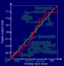
FSR defines max input signal for ADC.
The first transition should occur when input analog signal reaches a level of 1/2 LSB.
The offset error is a deviation from that level. The good news about this error is that it can be easily adjusted on the board, the bad news is that
the offset error drifts with temperature and time.
Gain error is also expressed in terms of LSB and represents the difference between the ideal and actual
output when the converter input is at full scale.
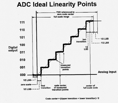
It can be confusing to determine ADC endpoints, FSR and LSB size. Remember, that we are taking measurements between
transition points, indicating that the converter output is in transition between one code to the next adjacent code.
The drawing below shows the transition points in the center of each step (there is a range of input values between each transition point,
that will produce the same ADC ouput code).
First we calculate the LSB weight: LSB=(Vfst-Vzst)/(2^Nbits-2), where Vfst- input signal resulting in full scale output code transition, Vzst- input signal resulting
in zero scale output code transition.
Offset error=Vzst - 0.5LSB. Subtracting 0.5LSB puts the point at the code center.
FSR=Vfst-Vzst+2LSB
Gain error=FSR - FSR_ideal
On the very first picture the green staircase belongs to an ideal ADC, red color reflects a real life case. Note, that a code width of the red curve differs
on each step - that is DNL error represents differences in analog input between adjacent steps in the staircase waveform.
Apparantly, if the DNL error is more than +/-1LSB, you may see missing codes on the diagram.
Again, to measure DNL we compare adjacent steps with the ideal (1LSB) step, unlike comparing pairs of adjacent steps between each other like some people suggest.
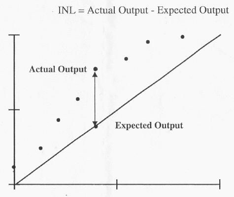
INL is the max deviation between the ideal and the real approximation lines on the diagram.
One of the known technique to measure DNL and INL is a histogram test. It requires a ramp signal applied to the ADC input, and
the ramp signal should consist of small steps, much smaller than 1LSB. For example if we apply 16 input steps per each ADC output step
we should see 16 output codes of the same value on the output of ADC, then another 16 equal output codes and so on. But this is in ideal case, real device
may have the number of codes different from 16 depending on where the transition occured. For our example if one particular ouput code
has 17 codes instead of 16, the DNL=(17-16)/16=1/16LSB. DNL has to be calculated for all codes.
INL=Integral sum of all DNL values.

SFDR,dB is the ratio of the fundamental frequency's amplitude to the largest spurious signal in the given
bandwidth.
THD,dB is the ratio of the rms sum of the first six harmonics to the amplitude of the fundamental frequency.
SINAD,dB is the ratio of the rms signal amplitude to the mean value of the root-sum-squares of all other harmonics
but excluding DC.
ENOB stands for effective number of bits and can be simply calculated from the formula: ENOB
= (SINAD-1.76dB)/6.02
SNR,dB is similar to SINAD, but excluding the first five harmonics and DC.
Testing the AC parameters
Testing of AC parameters of ADC is conducted with periodic signals (sine waves for example) and implies some limitations.
1. the set of samples representing the sine wave on the input of ADC should be COHERENT, meaning the following conditions should be met.
M/N = Ft/Fs, where
M - number of periods
(must be an integer)
N - number of samples
(must be a power of 2 for using an FFT algorithm)
Fs - sample rate
Ft - signal tone frequency
2. Fs/Ft>2, meaning the sampling frequency should be more than twice of the signal being sampled (Nyquist limit).
3. the two conditions above only make sense for periodic signals.
Along with M,N,Ft,Fs there are some more terms :
UTP=M/Ft=N/Fs - a unit test period, time required to take all samples.
Fres=1/UTP
- is the primitive frequency, which produces exactly one cycle within the UTP. Since all frequencies
resulting in coherent sampling must complete a whole number of cycles within the UTP, this means they must all be multiples
of Fres.
Frequency bins - discrete frequency spectrum components, harmonics.
For example, bin0 is the DC component, bin1 is Fres. For a set of N time domain samples there will be corresponding set of N/2 frequency domain bins, because
every frequency bin has 2 components (magnitude and phase). The magnitude and phase are coming from the time domain representation of
a sine wave signal: Vt = sin(2¶ft).
Problems associated with sampling
ALIASING - from the Nyquist sampling theorem, more than two samples per cycle of the input data
bandwidth required to avoid a loss of information. The aliasing error, caused by an insufficient sampling rate is
illustrated below.
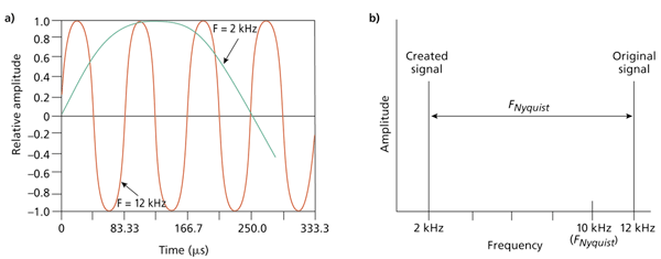
The picture illustrates 12kHz sine wave signal sampled with rate of 20ksamples/sec. Due to undersampling instead of 12kHz
signal now appears an alias at 2kHz as a difference of the original signal and the half of the sampling frequency.
Another source of aliasing error is in the spectrum of the sampled signal, causing replication of frequency components
Ft and Fs. For example, if Fs=5Mhz and Ft=2Mhz, an alias frequency Fs-Ft=3MHz will appear.
To remove this type of aliasing a low pass filter is required prior to the sampling stage to prevent high frequency
noise on the signal line from being aliased with sampling frequency, contaminating the resulting signal.
References:
- Mixed signal testing class
- ITC mixed signal testing
- http://www.national.com, http://www.maxim.com,http://www.linear.com
|