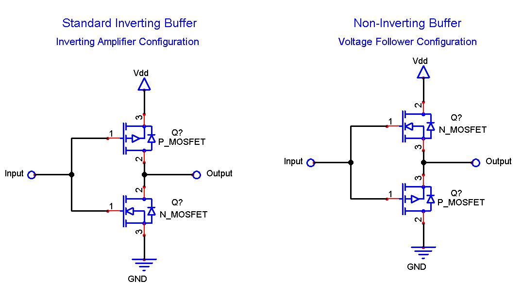
Q:
I swapped the transistors in CMOS inverter (put n-transistor at the top and p-transistor
at the bottom).
Can I use this circuit as a non-inverting buffer?
A:
Dear Hitequest,
First off, I'd like to thank you for hosting an excellent
website which has been very useful to me. Great work!
I have a question about the solution about the noninverting
buffer.
I didn't quite understand this because I thought the source
and drain were interchangeable depending on which one is at
a higher potential.In the case of NMOSFET, if one of the 2
terminals is tied to VDD,then, doesn't that become the
drain since it is at a higher potential?
I'd really appreciate if you could enlighten me on this
whenever you get time.Thank you and have a great day:-)
Thanks,Sriram
---------------------------
I still am not clear with one thing.
Perhaps,I should rephrase my question:
Consider the swapped circuit with NMOS on top and PMOS below.
One terminal of the NMOS is connected to Vdd(this becomes the
drain due to its higher potential).The gate is connected to Vdd
as well.So shouldn't it act like a pass transistor and conduct
current? there is a voltage difference between source
and drain since drain is connected to Vdd,right?
I'm really curious to know the answer.Thanks for your time and
have a great day:-)
Thanks Sriram
---------------------------
High input level is not enough to open NMOS transistor,
because it's source has the same high potential (Vdd) as a gate.
By the same reason low level will not open p-transistor.
Take care.
al
---------------------------
Hi Al,
Once again,thanks for responding immediately.I don't know what
I'm missing but how is the Vs of the NMOS equal to vdd/2.
I thought the source of the NMOS is basically the output node
of the new arrangement and its source voltage is indeterminate
at the beginning.Look forward to your reply.I appreciate your help.
Cheers
Sriram
---------------------------
hello Sriram,
if both transistors are closed,the output is close to tristate,
which is Vdd/2 (think about these transistors like of 2 large
value resistors).If you apply "1" to n_mos transistor, it is
to open , and it's Vs would be close to Vdd.
But it can't happen, because the Vg is not high enough.
al
Peter:
This configuration will indeed work as a current regulated
noninverting buffer. The assumption that both transistors
will be in cut-off is incorrect. A high will place the upper
MOSFET in a standard current source configuration and a low will
make the lower MOSFET a current sink.
The output will function as a current sink or source depending on
the input.
It is quite safe to assume that the gate threshold for transistors
in a CMOS device will be well below 1/2 Vcc when they are required
to be near saturation at 2/3 Vcc. The output swing will be reduced
by the gate threshold level (likely around 0.8V from either supply
rail with no load and having good current regulation for voltages
greater than 2V from rail).
It will not meet CMOS output specifications but it will be
a noninverting “soft” buffer.
Alex:
I agree with you that the assumption of both transistors being in
cut-off mode (Inverting buffer question) may be incorrect. Spice
tells they can sink/source some current , but the circuit can't
work as a non-inverting buffer, not even a "weak" one.
-------------------
Peter:
I must differ with you on this question however.
The output of a CMOS buffer that has the P-channel and N-channel
transistors swapped will be a non-inverting buffer with the output
voltage limited from reaching either supply rail by the gate
threshold voltage. Each transistor will be in a follower
configuration rather than being an inverting amplifier.
I was mistaken about the current limiting aspect. I was thinking of
J-FETs in that configuration but MOSFETs will provide full output
current. I assembled the circuit just to measure the actual
performance and it does function.
I didn't have any logic level TO-92 MOSFETs so the
minimum supply voltage was around 6 volts but it does work just fine.
Thank you for responding. I appreciate the dialog but again there
is no urgency on hypothetical situations.
-----------------------
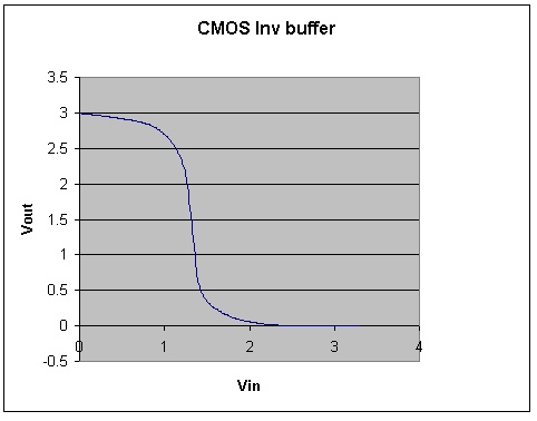
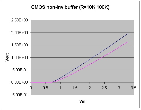
Alex:
Below there are Spice setup files and simulation results
(Vin/Vout plots) for both inverting and non-inverting buffers.
The plots show that the non-inverting circuit can sink and source
some current,but doesn't have the sharp switching characteristic
like an inverting buffer.
Peter's empiric results, however, tell the non-inverting buffer
does work.
Could that be a mismatch between simulation and lab results?
*CMOS NON-INVERTER
*P and N type devices swapped, bulk nodes connected to output
.MODEL NFET NMOS(LD=0.12u VT0=0.7)
.MODEL PFET PMOS(LD=0.12u VT0=-0.7)
Vdd 1 0 DC 3.3V
Vin 2 0 DC 0V
M1 1 2 3 0 nFET (L=2.2u W=91.3u)
M2 3 2 0 1 pFET (L=2.2u W=91.3u)
R1 3 0 10k
.DC Vin 0V 3.3V 0.1V
.PRINT DC V(3)
.END
Yuri M, principal device engineer at National Semiconductor :
My opinion is that the output of the non-inverting buffer will follow
the input level, but I wouldn't
recommend this circuit as a noninverting buffer.
Try to analyse the circuit with the input signal slowly rising
from GND to VDD.
Transistors should switch from open to close state. The
conditions for fast switching are worse for transistors of the non-inverting
buffer.
That means longer time interval when both transistors are open which may result
in short circuit and possible damage of the transistors.